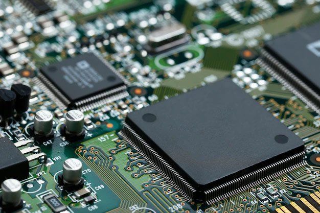
Advanced PCB
Advanced PCBs are commonly used in high-precision electronic devices. With the continuous development of technology, the demand is also getting higher and higher. To this end, the separate advanced PCB production workshop is opened to assist our customers achieve the best possible time to market and competitive advantage by producing PCBs in a sustainable way at the lowest total price through our fabrication capabilities, delivery punctuality and product quality.
Factory Scale
AlteraFlex's high-quality PCB R&D and manufacturing base (including the cooperative factory) is located in Shenzhen, China, with a plant area of 80,000 square meters and professional technicians accounting for 35% of the total number. It specializes in high-end prototypes, quick turn and small volume hardware designing and manufacturing services.
Such aspects should be borne in mind when comparing PCB prices. Reliability and a guaranteed/long life cycle involve an initially higher outlay, but will pay for themselves in the long run.
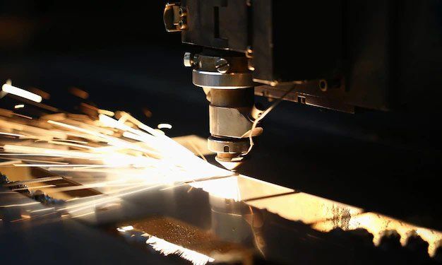
Laser Drilling
Minimum aperture up to 0.1mm for high-density interconnection (HDI) build-up multi-layer PCB, with electrical conduction between wirings on each layer controlled through interlayer vias. Currently laser drilling machines are extensively applied in processing of the Interlayer via-holes.
PCB Via Hole Plugging
Via Fill is a special PCB manufacturing technique used to selectively and completely close via holes with epoxy. There are many instances in which a PCB designer might want to have a via filled.
Some key benefits are:
More reliable surface mounts
Increased assembly yields
Improved reliability by decreasing the probability of trapped air or liquids.
Plating Through Holes
Real-time monitoring of chemical quality in copper plating sinks. The aim of electroless copper is to plate a conductive layer through a hole or into a blind microvia.
Vacuum Etching
Using the vacuum etching technology to make sure that both surfaces of the board are very uniform. it produces a straighter conductor profile, allowing the resulting plate to more accurately match the wiring requirements.
Proven Technology
Professional R&D on high-density HDI, multi-layer PCB, rigid-flex PCB. Embedding technology of small size core, PCB with special requirements from industries like Telecom / medical/automotive, etc.
Qualified Materials
Sourcing high-quality materials from Rogers, Shengyi, Wazam, Dupont, Rohmhass, Atotech, and other excellent suppliers to choose the best ones. Widely used in communications, industrial control, computer applications, medical, test equipment, and other fields.
Independent Production Line
When you order advanced PCBs from AlteraFlex, you are buying quality that pays for itself over time. In the comparison chart below you can see where the advanced PCB is unique or goes beyond the IPC standard.
Application Area
Advanced PCB is widely used in communications, industrial control, computer applications, medical, test equipment and other fields. The core competitiveness: leading technology, high quality, high precision rate, expedited delivery, consultative customer service, and optimal cost performance. With ISO9001, ISO14001, TS16949, UL, RoHS certification.

5G/4G, wireless communication, digital TV, mobile phone, fiber optic communication, communication equipment, radio frequency, Bluetooth, radio.
The consumer electronics industry demands high performance technology to be complex and compact at the same time.
Industrial instrumentation, sensors, robots, automation, motors, internet of things.

The medical field requires a vast level of technology with extreme reliability and long term life cycles.
3D printing, mobile medical, internet +, medical equipment, wearable, telemedicine.
The automobile industry must have circuit boards that are extremely reliable with an emphasis on safety.
Electric vehicles, automotive electronics, new energy vehicles, car networking, automotive electronics, body electronics, powertrain, automotive safety.
| ADVANCED PCB | STANDARD PCB | |
|---|---|---|
| Item | HIGH-END,COMPLEX Ideal If You Need A High-end, Complex PCBS | INEXPENSIVE , FAST Ideal If You Need A Inexpensive, Quick-turn PCB |
| Application | Industrial equipments, instrumentation, automotive electronics, communication equipments, etc. Finished products require high reliability and stable quality for users | Children's toys, small appliances, home lighting, functional testing, electronic enthusiasts, etc. Suitable for users whose prices are core competitiveness |
| Engineering | ✔ Senior engineer (one file/6 hours) | ✔ Mid-level engineer (5 files/hours) |
| Production | ✔ individual working panel | ✔ mixed working panel |
| Quantity | ✔ ≥1 piece | ✔ 5,10,15,20,25...pieces |
| Material | ✔ Shengyi,Rogers,Arlon,Isola,Omega,Nelco,3M etc. | ✔ KB(kingboard)/GDM(goldenmax) |
| Ink, Soldermasks | ✔ Meet IPC4101 class B/L | ✔ Meet IPC4101 class B/L |
| drilling | ✔ Rohm&Haas,TAIYO,Kuangshun,Meet IPC-SM-840 class T | ✔ TAIYO,Kuangshun,Meet IPC-SM-840 class T |
| plating | ✔ Min Mechanical Hole Size 0.15mm,Laser hole 0.1mm | ✔ Min Mechanical Hole Size 0.2mm |
| Soldermask offset | ✔ PTH (Hole copper thickness≥20um),IPC 3(25um) | ✔ PTH(Hole copper thickness≥18um) |
| Dimensional | ✔ ±2mil | ✔ ±3mil |
| deviation | ✔ ±0.13mm | ✔ ±0.2mm |
| Warping angle | ✔ 0.75% | ✔ 1% |
| Test method | ✔ A.O.I,Kelvin Four-terminal sensing,Microsection Inspection,Solderability Test,Impedance Test... | ✔ A.O.I.,Fly Probe Testing |
| Glass transition ℃ | ✔ >140℃ | ✔ >130℃ |
| Package | ✔ Humidity indicator cards | None |
| Inspection report | ✔ Inspection report | None |
| Standard | ✔ IPC Class 2,IPC Class 3,Automotive Standard,Customer Standard | ✔ IPC Class 2 |
| Etched line | ✔ Forbid to repair tracks(IPC 3,Automotive,Customer Standard) | - |
| Cleanliness | ✔ Cleanliness requirements beyond those of IPC | ✔ Meet IPC standards |
| Certification | ✔ UL,ISO9001:2008,ISO14001:2004,ISO/TS16949:2009,RoHS etc. | ✔ UL,ISO9001:2015,RoHS etc. |
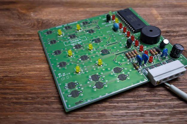
High-quality PCBs Showcase